wordpress-seo domain was triggered too early. This is usually an indicator for some code in the plugin or theme running too early. Translations should be loaded at the init action or later. Please see Debugging in WordPress for more information. (This message was added in version 6.7.0.) in /var/www/reachemchemicals.com/blog/wp-includes/functions.php on line 6170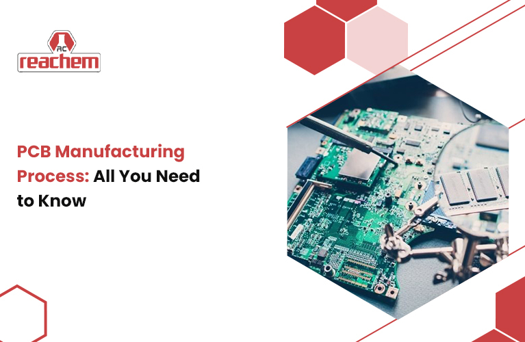
Reachem
As someone who loves gadgets and electronics, you might wonder how those intricate circuit boards come to life. Well, you’re in the right place. In this blog, we’ll walk you through the entire PCB manufacturing process from start to finish. Whether you’re a tech enthusiast or just curious, this guide will be both informative and engaging. Let’s dive into the fascinating journey of creating a printed circuit board (PCB) that powers our favorite devices.
A printed circuit board (PCB) is a flat board that connects electronic components using conductive pathways. PCBs are the backbone of most electronic devices, providing a foundation for electrical connections and mechanical support. With PCBs, modern electronic gadgets would function more efficiently and reliably.
There are various types of PCBs, each designed for unique applications. Here are some common types:
Each type has its benefits, making it ideal for particular applications.
The first step in PCB manufacturing is designing the circuit layout. This involves creating a blueprint that guides the entire process. Key steps are:
A well-thought-out design ensures the PCB will function correctly and be manufacturable.
Choosing the right materials is crucial for the performance and reliability of the PCB. Key materials are:
Selecting high-quality materials ensures the PCB will perform well under various conditions.
Once the design is finalized, it’s time to transfer it onto the PCB. Key steps are:
Printing the design accurately is essential for the PCB to function as intended.
Etching removes the unwanted copper, leaving behind the desired circuit pattern. Key steps are:
Proper etching ensures the copper traces are clean and well-defined.
Drilling creates holes for component leads and vias that connect different layers. Key steps are:
Accurate drilling is vital for component placement and electrical connectivity.
Plating adds a layer of metal to the holes and traces, improving conductivity. Key steps are:
Plating is essential for creating reliable electrical connections.
The solder mask protects the copper traces and prevents short circuits during soldering. Key steps are:
A good solder mask application enhances the durability and reliability of the PCB.
Silkscreen printing adds labels, logos, and other important markings to the PCB. Key steps are:
Clear silkscreen markings help in the assembly and troubleshooting of the PCB.
Applying a surface finish protects the exposed copper and improves solderability. Common surface finishes are
Choosing the right surface finish ensures the PCB’s longevity and performance.
The final steps involve assembling the components and testing the PCB to ensure it works. Key steps are:
Thorough assembly and testing guarantee that the PCB functions correctly in its final application.
And there you have it—a comprehensive guide to the PCB manufacturing process. From design and material selection to assembly and testing, each step is crucial for creating a reliable PCB. Understanding this process helps us appreciate the complexity and precision involved in making the electronics we use daily. We hope you found this journey through PCB manufacturing both informative and engaging. Whether you’re a tech enthusiast or just curious, knowing how these tiny yet powerful boards come to life is truly fascinating.


